Research
We investigate the optical and electrical properties of compound semiconductors, oxide materials, and other exotic materials such as graphene, perovskites, and quantum dots for optoelectronic and energy device applications. We improve the performance of energy and optoelectronic devices by using nano-size effect, surface plasmon, photonic crystal, band gap engineering, ohmic contact, and device simulation for device applications to light-emitting diodes, sensors, solar cells and other energy-related devices.
1. GaN Materials and Devices
GaN and its alloy with Al and In recently became the basic materials for short-wavelength optoelectronics and high speed transistors. This was due mainly to their direct energy gaps covering the whole visible spectrum and a large part of UV range (6.2, 3.4 and 1.9 eV for AlN, GaN and InN respectively).
• High thermal conductivity
• Wide bandgap energy
• High breakdown field and electron mobility
These general properties lend themselves to exploitation in nearly any electronic and optical device with special applications in high power electronics, high frequency applications, and use in hostile conditions such as high temperature probes.
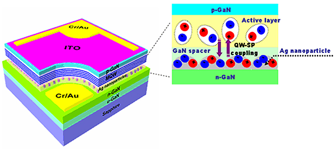
Surface plasmon-enhanced InGaN-based LEDs
Surface plasmons (SPs) have attracted much attention because optical properties can be greatly enhanced by coupling between SPs and the multiple quantum wells (MQWs) in LEDs. SPs are the collective oscillations of free electrons in a metal at the interfaces between metals and dielectrics. Especially, surface plasmon polaritons (SPPs) at metal surfaces and localized surface plasmons (LSPs) of metallic nanostructures can both be used to enhance the spontaneous emission rate and internal quantum efficiency of LEDs.
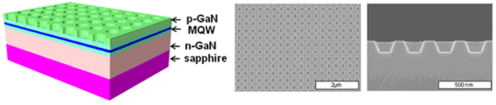
Photonic crystals
Photonic crystals (PCs) are periodic dielectric structures that have a band gap that forbids propagation of a certain frequency range of light. LEDs with PCs could be designed to efficiently couple light from the dielectric-guided modes into air. They can be utilized to inhibit emission of guided modes or redirect trapped light into radiated modes.
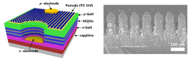
Antireflective sub-wavelength structure (SWS) is an ordered or disordered tapered feature with gradient refractive index. When the grating period becomes smaller than the wavelength, all higher-order diffracted fields are evanescent and only the zero-order propagates. At this time, the SWS can be regarded as a homogeneous medium with effective refractive index.
High-power LEDs with improved efficiency droop
As the efficiency of LEDs improves, LEDs find more applications such as back light unit, automotive headlights, and general illumination. However, as injection current increases in InGaN/GaN MQWs LEDs, we observe a unique phenomenon called "efficiency droop" that is the reduction in LED efficiency at high injection current density. Therefore, the efficiency droop should be solved to develop the high-power LEDs.
Research results in GaN photonic devices
Surface plasmon-enhanced InGaN-based LEDs
We demonstrated the SP-enhanced InGaN/GaN MQWs blue LED with silver nanoparticles inserted into the n-GaN or the p-GaN layer of LEDs because the enhancement of local electromagnetic fields is strongly dependent on the distance between the MQWs and the metal nanoparticles. The internal quantum efficiency and optical output power of LEDs were significantly improved by the coupling between exciton dipole in MQWs and SPs. Furthermore, we developed SP-enhanced green and ultraviolet LEDs by using gold and platinum, respectively.
Enhanced light extraction from GaN-based LEDs with Photonic Crystals and Nanostructures
We reported the development of GaN-based LEDs with PCs, which was formed inside p-GaN or n-GaN layer with SiO2 pillar and outside the p-bonding electrode on p-GaN layer. As a result, the optical output power was greatly enhanced by PCs compared to that without PCs. In addition, we also confirmed that internal quantum efficiency was increased by PCs which were embedded p-GaN or n-GaN layer.
We also reported the light extraction efficiency of LEDs with ITO SWS dependent on the periodicity. Compared to the light output power of LEDs with flat ITO, the light output powers of LEDs with non-periodic and periodic ITO SWS were increased by gradient refractive index of SWS. In addition, we reported that the light output power of LEDs with periodic ITO SWS was higher than that of non-periodic ITO SWS. This indicates that periodic ITO SWS has more perfect gradient index profile.
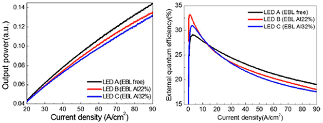
High-power LEDs with improved efficiency droop
In order to improve the efficiency of LEDs, the electron blocking layer (EBL) has played an important role in effectively confining electrons in the MQWs region of LEDs. We investigated the effect of the p-AlGaN EBL on efficiency droop in InGaN/GaN MQWs LEDs. At the low current density, LEDs with an EBL show a higher EQE than LEDs without an EBL. However, LEDs without an EBL show a higher EQE at high current density. The suppression of efficiency droop in LEDs without an EBL at high current density is attributed to an increased hole injection efficiency.
2. ZnO Materials and Devices
In the upcoming information, digital, and multimedia age, light-emitting diodes (LEDs) based on wide-bandgap semiconductors have drawn much attention. The high efficiency, fast switching time, high color gamut, low power consumption, semipermanence, and low heat output of the LEDs have led to many new applications. The backlight units in liquid-crystal displays have been replaced by high-efficiency LEDs. As the efficiency of LEDs was further improved, many products equipped with LEDs have been reported. To meet the requirement of high-brightness LEDs for illumination, mobile appliances, automotive, and displays, it is necessary to develop new wide-bandgap semiconductors such as ZnO, which has excellent structural and physical properties compared to GaN.
Basic properties of ZnO
Zinc oxide (ZnO) is a II-VI compound semiconductor with a hexagonal wurtzite structure. Recently, ZnO has attracted much attention for its application in various fields such as UV light-emitting devices, varistors, transparent high power electronics, optical waveguides and solar cells. In particular, ZnO has been considered as promising materials for short-wavelength optoelectronic devices because it has a direct bandgap of 3.3 eV and a low threshold voltage. ZnO also has a number of advantages over GaN, the wide-bandgap semiconductor currently utilized in the short-wavelength optoelectronics industry. Some of these advantages include a large exciton binding energy (~ 60 meV), a higher radiation hardness, simplified processing due to amenability to conventional chemical wet etching and the availability of large area substrates at relatively low material costs.
ZnO epitaxial film
It has been compelling research attention for a long time because of its applications in many scientific and industrial areas such as piezoelectric transducers, optical waveguides, acousto-optic media, conductive gas sensors, transparent conductive electrodes, and varistors. It has now received increasing attention and is recognized as a promising candidate for applications related to its optoelectronic possibilities in the UV range. Furthermore, its piezoelectric properties could allow the development of SAW filters to be integrated in future analog circuits for portable electronics for which there is a strong need.
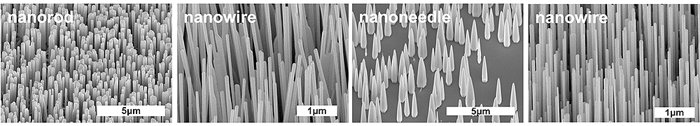
ZnO-based 1-dimensional nanostructure
ZnO nanostructure can be easily produced by several growth techniques because ZnO have the preferred c-axis orientation due to the minimal surface energy in the ZnO wurtzite structure. The 1 dimensional (1D) ZnO nanostructures which include highly ordered nanowire arrays, nanorods, and nanobelts are promising candidates for nano-electronic and photonic. 1D ZnO nanostructures are found to be highly suitable for nanoscale applications such as room temperature laser, field effect transistor, nanoresonator, etc.
Research results in ZnO devices
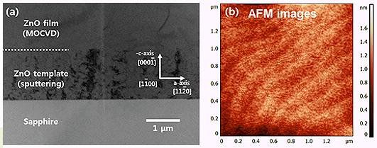
Epitaxial growth of ZnO film
It has been reported that the ZnO-based LEDs can be grown by growth methods based on physical vapor deposition (PVD) such as molecular beam epitaxy, pulsed laser deposition, and sputtering. However, because of disadvantages of PVD such as low growth rate, small area growth, difficulty of alloy growth and sophisticated and expensive ultra-high vacuum equipment, it is difficult to commercialize the ZnO based LEDs. In the early stage of commercialization of ZnO based LEDs, metalorganic chemical vapor deposition (MOCVD), is very important, because MOCVD has many advantages for the industrial applications such as its high deposition rate, large area and high quality epitaxial growth. However, because of difficulty of growth of epitaxial ZnO film and p-type ZnO film, ZnO based devices grown by MOCVD have shown the intense deep-level emission peaks along with very weak UV emissions. Recently, we reported on the evolution of the surface morphology and the change in the growth mode from three-dimensional to two-dimensional by controlling VI/II gas ratios, resulting in the improvement of the structural, morphological, and optical properties ZnO films.
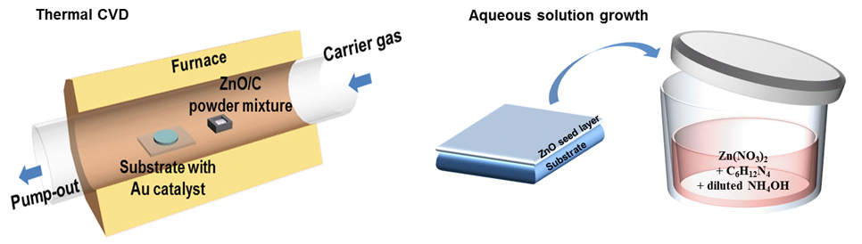
Growth of ZnO nanostructures
There are several methods to grow the ZnO nanostructures. These growth methods are based on two mechanisms: (1) vapor phase growth and (2) solution phase growth. Methods for vapor phase growth and solution phase growth are diverse techniques including thermal CVD, direct thermal evaporation, MOCVD, electrochemical deposition, and aqueous solution growth, etc. In our group, growth methods using thermal CVD, MOCVD and aqueous solution are well-organized to synthesize the high-quality ZnO nanostructures.
ZnO-based homojunction LEDs
UV LEDs and LDs are of interest for their potential use in long-lifetime solid state lighting, high-density information storage, secure communication, and chemical/biological agent monitoring. The commercial availability of large-area ZnO substrates and the possibility of performing wet etching make the fabrication of ZnO-based optical devices an attractive prospect, as it would enable the fabrication of vertical-geometry devices with low threading dislocation densities by a simple process. We reported the UV electroluminescence emission from ZnO-LEDs grown by RF-Sputtering method. We have investigated the ZnO-based LEDs and tried to improve the emission efficiency of ZnO-based LEDs by using MOCVD growth method.
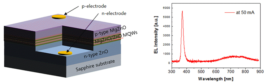
ZnO-based heterojunction LEDs
To enhance the efficiency of GaN-based LEDs, it is necessary to replace p-GaN layer with a p-type semiconductor layer which has high hole concentration, as well as appropriate structural and optical properties. The p-type ZnO with high hole concentration above ~ 1018 cm-3 can be produced by MOCVD growth. The p-type ZnO can be used as a hole supplying layer by replacing the p-GaN in GaN LEDs. In addition, the ZnO refractive index of 2.0 is smaller than the GaN of 2.4, allowing an increase in the probability of photon escape in the heterojunction LEDs. Heterojunction LEDs using p-ZnO on InGaN/GaN MQW are expected to have several advantages in electrical and optical properties over the conventional GaN LEDs.
Transparent conducting oxide (TCO)
In most optoelectronic devices such as flat panel displays, LEDs, and solar cells, it is essential to use a transparent electrode such as a thin film transparent conducting oxide (TCO). ZnO-based TCOs have attracted significant attention due to their good conductivity, high optical transparency (in the 90% range), excellent surface smoothness, low deposition temperature, good etch-ability for patterning, good reproducibility, inexpensive and abundant binary compound material. There are many reports on TCO semiconductors based on ZnO such as aluminum doped zinc oxide (AZO), gallium-doped zinc oxide (GZO), indium-doped zinc oxide (IZO), tin-doped zinc oxide (TZO) in large part. Our group has been working in growing the high quality ZnO TCO film and applying the film to LEDs and solar cells as a transparent electrode.
ZnO nanostructure devices and solar cells
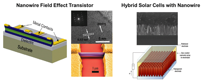
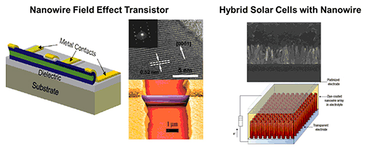
1D nanostructures, such as nanowires, nanobelts, and nanowalls provide a good system to investigate the dependence of electrical and thermal transport or mechanical and optical properties. Nanowires are the smallest dimensional structure with high crystallinity that can efficiently transport electrical carriers. Therefore, many researchers can be exploited to make a number of nanoscale devices such as field effect transistors, emitting devices, sensors, photovoltaic devices, memory devices, and logic circuits. Especially, ZnO nanowires have received considerable attention due to their unique properties, such as a wide direct bandgap (~3.37 eV), a large exciton binding energy (~60 meV), and piezoelectricity. Also, the large surface area to volume ratio of ZnO nanowires has a strong influence on electrical transport properties with surrounded elements. As a result, nanowire FETs are suitable for the understanding of the electronic transport mechanisms with surface interface roughness, size and shape of the ZnO nanowire. In addition, to date, hybrid solar cells incorporated with nanowire array structure have the advantages with efficient light-harvesting and direct electrical pathways for electron-hole pairs. We focused on the field of field effect transistors and solar cells.
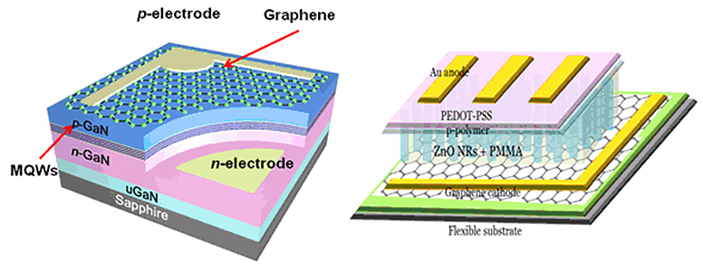
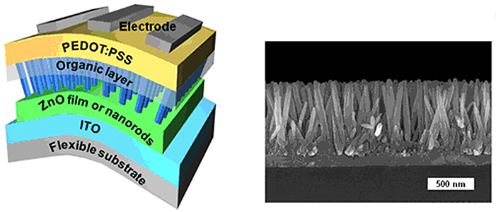
Hybrid ZnO/organic devices
As an alternative approach to the ZnO p-n homojunction LEDs, we have been working in fabricating p-n heterojunction LEDs by introducing organic semiconductors as p-type materials due to the lack of reliability and reproducibility of p-type ZnO. The hybrid materials promise good properties by combining the advantages of both materials such as high flexibility of polymers with the structural, chemical, and high functional stability of inorganic materials. In addition, ZnO can be easily synthesized to one-dimensional nanostructures by using CVD and hydrothermal methods. The ZnO (nanostructures)/organic hybrid structures may lead to various applications in optoelectronic devices such as LEDs, solar cells, and flexible electronics.
3. Flexible Semiconductor Devices
Flexible GaN-based LEDs
GaN-based LEDs have been greatly advanced in fabrication and performance, so they have extended their application fields to general illumination and displays. Nevertheless, there remain another opportunities for flexible, foldable, and stretchable applications. GaN-based LEDs are generally fabricated on sapphire substrates due to the quality and cost, so that GaN-based LEDs should be separated from the rigid sapphire substrate for flexible formats. Therefore, we study the fabrication process including LED lift off process and printing process with GaN-based LEDs grown on a sapphire substrate to realize flexible GaN-based LEDs.
Nano devices and solar cells using ZnO nanostructures
1D nanostructures, such as nanowires, nanobelts, and nanowalls provide a good system to investigate the dependence of electrical and thermal transport or mechanical and optical properties. Nanowires are the smallest dimensional structure with high crystallinity that can efficiently transport electrical carriers. Therefore, many researchers can be exploited to make a number of nanoscale devices such as field effect transistors, emitting devices, sensors, photovoltaic devices, memory devices, and logic circuits. Especially, ZnO nanowires have received considerable attention due to their unique properties, such as a wide direct bandgap (~3.37 eV), a large exciton binding energy (~60 meV), and piezoelectricity. Also, the large surface area to volume ratio of ZnO nanowires has a strong influence on electrical transport properties with surrounded elements.
Hybrid ZnO/organic devices
Recently, a few researches have been performed in fabricating p-n heterojunction LEDs by introducing organic semiconductors as p-type materials due to the lack of reliability and reproducibility of p-type ZnO. This is the good method as an alternative approach to the ZnO p-n homojunction LEDs.
Growth of graphene and its application
Graphene has a large specific surface area, high thermal conductivity (~5000 W/m K), high intrinsic carrier mobility (21000 cm2/V s) at room temperature, high transparency (80%), and good mechanical stability. Its optical transmittance and good electrical conductivity draw attention for applications as transparent conductive electrodes.
Results in Flexible Semiconductor Devices
Flexible GaN-based LEDs
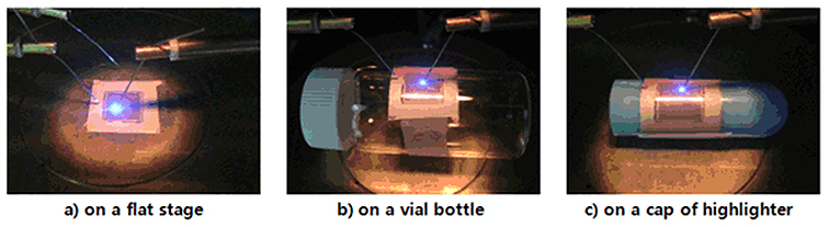
GaN-based LEDs are generally fabricated on sapphire substrates due to the quality and cost, and the GaN-based LEDs can be separated from the sapphire substrate by laser lift off process. Therefore, we have investigated a laser lift off process to transfer GaN-based LEDs onto a flexible PET substrate. GaN-based LEDs bonded on the PET substrate can be separated from the sapphire substrate by laser lift off process. After transferring LEDs onto flexible substrate, the LEDs are operated successfully. This result shows that proposed transferring method can be used to fabricate flexible GaN-based LEDs.
Nano devices and solar cells using ZnO nanostructures
Nanowire FETs are suitable for the understanding of the electronic transport mechanisms with surface interface roughness, size and shape of the ZnO nanowire. In addition, to date, hybrid solar cells incorporated with nanowire array structure have the advantages with efficient light-harvesting and direct electrical pathways for electron-hole pairs. We focused on the field of field effect transistors and solar cells.
Hybrid ZnO/organic devices
The hybrid materials promise good properties by combining the advantages of both materials such as high flexibility of polymers with the structural, chemical, and high functional stability of inorganic materials. In addition, ZnO can be easily synthesized to one-dimensional nanostructures by using CVD and hydrothermal methods. The ZnO (nanostructures)/organic hybrid structures may lead to various applications in optoelectronic devices such as LEDs, solar cells, and flexible electronics.
Growth of graphene on semiconductors and application